Author: Christian Radici, Applications Engineer, Manchester.
This interactive application note contains embedded Cloud based simulations to augment the text.
To open the embedded simulation, simply hover over the simulation image. Left click anywhere in the graphic area once the central play button changes in colour. This opens the schematic in the Cloud environment. See the interactive application note tutorial page for more details on how to use the simulations. See accompanying application note: AN50006.
Introduction
Power MOSFETs are extensively used as switches due to the very low RDSon and thus low conduction losses. However, in many applications MOSFETs are used in their saturated state, with certain cases requiring both these modes to be robust and performant within the same device.
This interactive application note aims to describe the main characteristics of linear mode operation from a theoretical standpoint. Nevertheless, application-oriented topics are discussed in case of HotSOA derating and pulse shape conversion. Example simulations are included in the relative paragraphs.
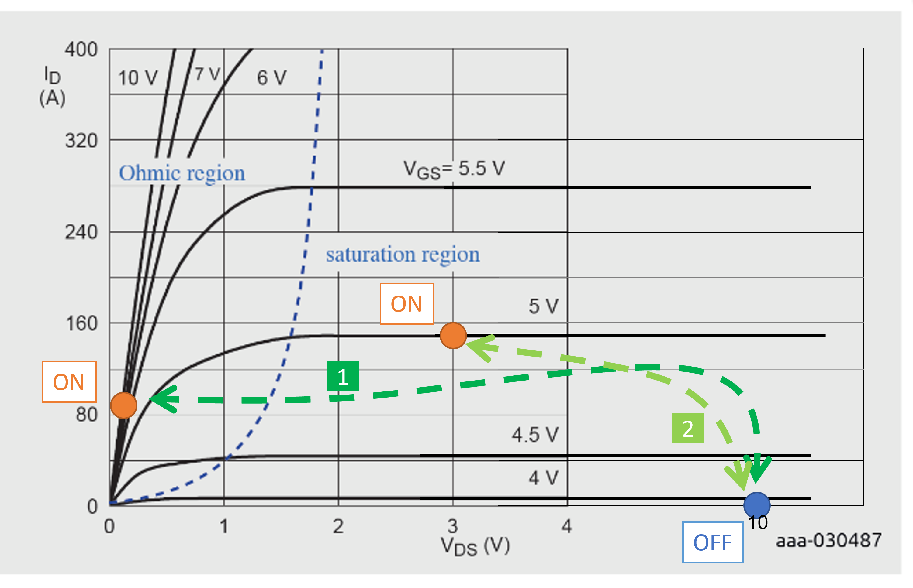
Figure 1. Example of MOSFET output characteristic ON/OFF trajectories
Linear mode definition
During linear mode a MOSFET operates in its saturated state, or saturation region, and it behaves as a (gate) voltage controlled current source. Contrary to what happens when fully ON (or fully enhanced), the drain-source impedance is relatively high, resulting in high power dissipation. In linear mode, the power is given by the product of the drain current and the drain-source voltage (ID × VDS), which are both high at the same time.
Linear mode can be described analytically by the set of equations below. The MOSFET needs to be ON (Equation 1) and the VDS greater than the overdrive voltage (VOD) (Equation 2). If the previous two conditions are met the drain current will be proportional to the square of VOD (thus the applied VGS) as shown in Equation 3, where k is a technological parameter fixed with the type of trench technology used.
(Eq. 1)
(Eq. 2)
(Eq. 3)
MOSFETs can operate in linear mode in two ways: indirectly, for a short time, as a consequence of switching or directly, for much longer time. In fact, linear mode is traversed every time a MOSFET switches ON and OFF. With reference to Fig. 1, during turn ON the MOSFET’s working point moves from high VDS and zero ID (OFF state) to a low VDS and high ID (curve 1). Certain applications require MOSFETs to purposely operate in linear mode (curve 2). In this case it is recommended to:
- Guarantee that the device operates within the SOA curve, for a given pulse duration and mounting base temperature (Tmb)
- Employ adequate thermal management techniques.
Examples of typical linear mode applications
Simulation 1 - Airbag applications
Simulation 1 - Airbag applications
Simulation 2 - Active clamp
Simulation 2 - Active clamp
Simulation 3 - Capacitor pre-charge (soft start / hot swap)
Simulation 3 - Soft start
Simulation 4 - LDO (low dropout) regulators
Simulation 4 - LDO regulator
SOA graph
The safe operating area (SOA) graph gives an indication of the amount of power a device can safely handle before failing. The graph shows the drain current plotted against the drain-source voltage. The limit depends on the time duration of the power and the working region the MOSFET operates in. The graph is valid only for a constant mounting base temperature of 25 ?C and either a single pulse or DC operation. The SOA is especially useful in case of linear mode operation. Fig. 2 shows the area below which a MOSFET can safely and reliably operate for a pulse of 1 ms and the limit at VDS = 3 V and pulse of 1 ms.
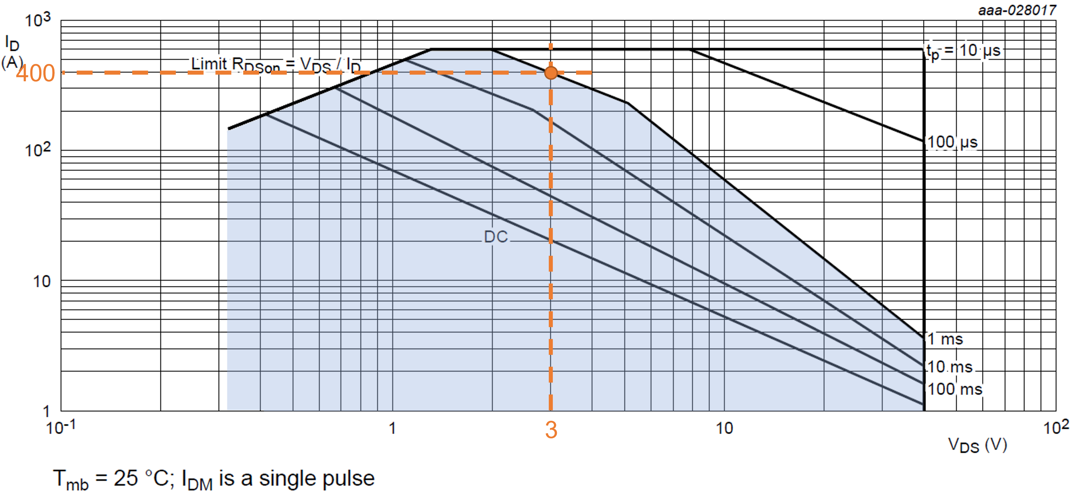
Figure 2. SOA maximum current limits for 1 ms and at VDS = 3 V and 1 ms pulse
Fig. 3 shows how the SOA graph can be subdivided depending on the MOSFET’s working region (a time pulse of 1 ms is considered).
- The yellow line corresponds to the limit in RDSon mode
- The green line indicates the limit imposed by the package
- The blue line shows the avalanche limit (at the maximum rated voltage, before avalanche occurs).
- The red line shows the limit during linear mode operation. This limit is verified experimentally by keeping VDS constant while the current is pulsed for a given duration. As shown in Equation 4, it depends on the thermal impedance of the MOSFET (Zth), maximum junction temperature (Tj(max) = 175 ?C) and mounting base temperature (Tmb).
For a more in-depth description of the SOA limits see AN11158 Understanding power MOSFET data sheet parameters (3.1 Safe Operating Area (SOA) curves).
(Eq. 4) 
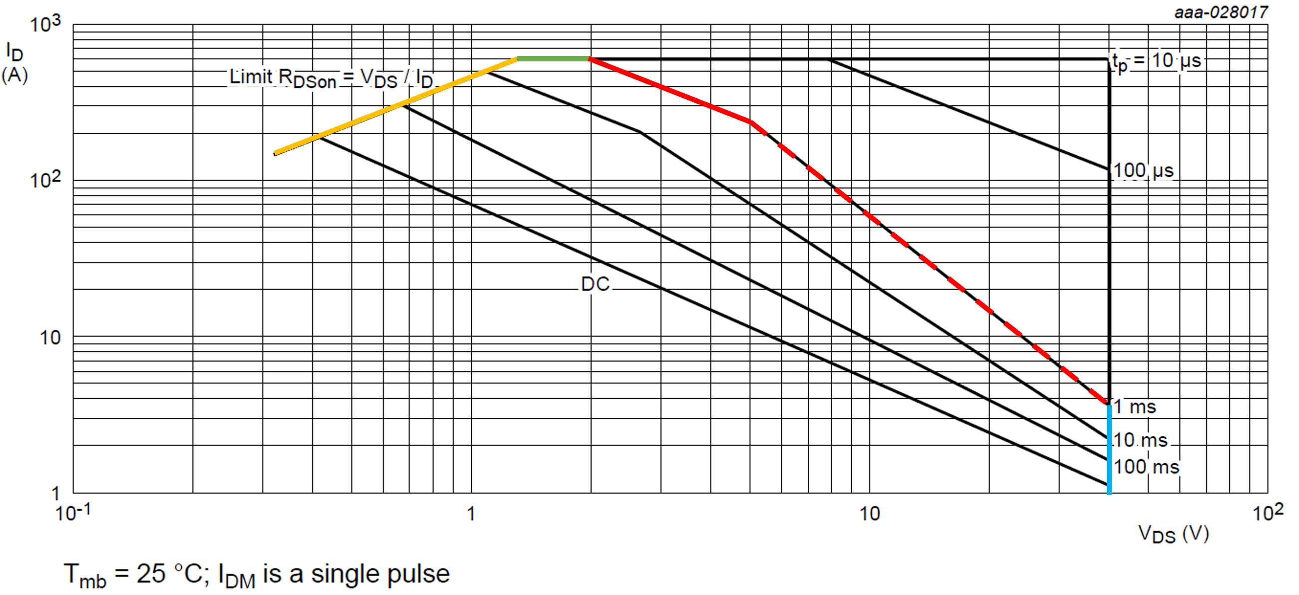
Figure 3. SOA graph; curve limits
From Equation 4 it follows that the limit increases (more power can be dissipated) as the time pulse decreases. Finally, the dashed red line indicates the Spirito region, where thermal instability occurs.
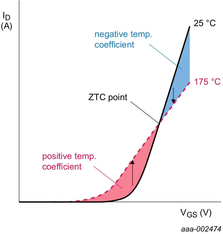
Temperature dependency
Thermal instability
For a fixed VDS, the variation of drain current against gate bias voltage is plotted in the transfer characteristic graph, shown in Fig. 4. Two lines are used to show the MOSFET operation at a junction temperature of 25 °C (solid line) and 175 °C (dashed line). For a low enough VGS, the MOSFET will conduct more current if it operates at 175 °C than at 25 °C, due to the negative temperature coefficient of the threshold voltage (VGSth), as shown in Fig. 5. In this case the MOSFET is operating in a region of thermal instability, identified by a positive temperature coefficient of the current. This holds true even when considering a single spot on the silicon die [1].
However, this phenomenon can be avoided. In fact, for a given VDS, there is a critical current above which there is a negative feedback and thus thermal stability. This is known as the Zero Temperature Coefficient (ZTC) point.
On the SOA graph, thermal instability is indicated by a two-slopes line and an additional inflexion point, as shown in Fig. 6 (the inflexion point is located at 5 V for a 1 ms pulse). The theoretical limit, in the dashed blue line, is calculated using Equation 4, where Zth = Zth(j-mb). This limit can be found using an RC thermal model, like the Cauer model shown in Fig. 7. The dashed red line indicates the real performance of the device. In this case Zth ≠ Zth(j-mb) and therefore the limit cannot be found using an electrical model. The reduction in performance can be quite severe: in this case for a VDS of 20 V, the maximum current the MOSFET can handle goes from a theoretical 60 A down to around 15 A (75% less). This phenomenon is also known as Spirito effect, and it is caused by the uneven distribution of current across the silicon die. Below the ZTC point, if a small region is at a higher temperature than the rest of the die, it will draw more current and dissipate more power becoming even hotter. This process eventually leads to thermal runaway and the destruction of the MOSFET as a three-terminal short. Burn marks will appear near the center of the die and close to the die bonding structure, as documented in AN11243 Failure signature of electrical overstress on power MOSFETs (1.3 Linear mode operation).
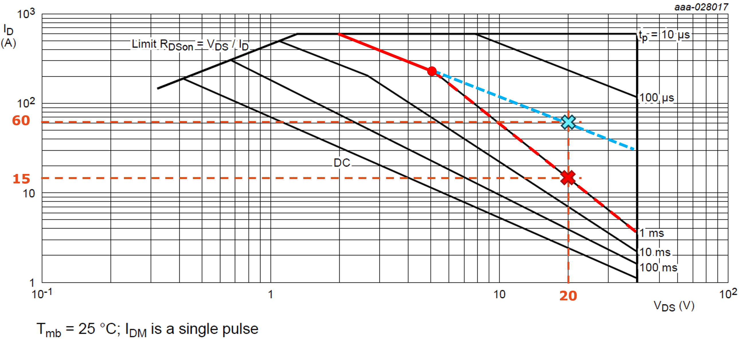
Figure 6. SOA graph: Spirito effect
Moreover, these hotspots are observed to occur more frequently at wider power pulses.
With reference to Fig. 6, for a time pulse of 10 ms the Spirito effect takes place at a lower VDS (around 3 V) than for the 1 ms pulse (5 V) while DC operation is limited by thermal instability at any voltage.
The uneven distribution of current across the silicon die is influenced by uniformity of the MOSFET cells and integrity and uniformity of the die attachment. Besides, the type of die bonding technology can also have a significant impact. As shown in Fig. 8, wire bonding increases current density in small points of the die that can become hot spots. On the other hand, the copper clip of an LFPAK prevents localised current crowding reducing the likelihood of hot spot formation.
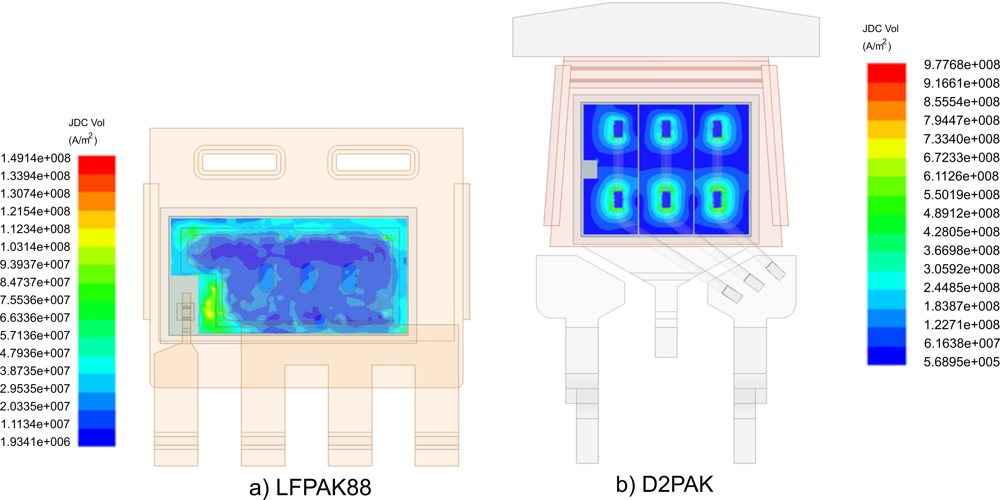
Note: current density contour scaling is different for LFPAK88 and D2PAK, see accompanying colour scaling
Also, cell density influences the shape of the SOA. Older trench (or planar) technologies show a higher RDSon, due to the wider cell pitch and thus lower cell density. For a given total drain current, cells in older technologies are more likely to operate beyond the ZTC point, where operation is thermally stable, since the current per cell is higher. Consequently, for a given die size, older trench (or planar) technologies show a higher RDSon but in turn perform better in linear mode.
The innovation introduced with new trench structures has deeply increased performances in some of the other fields, particularly in switching, avalanche and steady state behavior. Newer technologies show generally worse linear mode capability, however, whenever harder requirements have to be met the designer can either choose (in case the thermal design cannot be improved): a MOSFET with a lower Rth(j-mb) (corresponding to a bigger die), a bigger package, an older technology (with lower cell density) or a MOSFET from Nexperia’s ASFET portfolio with Enhanced SOA capability.
5.2. Hot-SOA derating
The SOA graph in Nexperia’s data sheets is valid only for a mounting base temperature of 25 °C. If the mounting base is held at a different temperature, then the graph must be derated, as generally the capability at other temperatures is not characterized. In this case, either an approximated or an exact indication of the new limit is found, depending on the device’s working region.
There are three main derating methods depending on which quantity is scaled or kept constant. If the current is scaled, then the voltage will remain constant, vice versa if the voltage is scaled, the current will remain constant. The third option is to scale both voltage and current thus keeping the power constant. The RDSon, package, breakdown and linear mode limits are all predicted in the same way by these methods. The only difference is in how the Spirito region is approximated, i.e. the position of the inflexion point. For a given VDS the current scaling method returns the highest limit, while the voltage scaling the lowest. Generally, when compared with a measured Hot-SOA every method is observed to underestimate the device’s real performance, which gives some safety margin from thermal instability. As shown in Fig. 9 the current scaling method usually gives the best Spirito approximation.
Figure 9. Example of SOA derating methods against measurement for the BUK7Y2R0-40H
Table 1 summarizes the current limits predicted using the three methods and measurement at VDS = 30 V, Tmb = 125 °C and pulse of 1 ms.
| ID limit: VDS = 30 V; Tmb = 125 ?C; pulse width = 1 ms | |||
|---|---|---|---|
| Measured | Current scaling | Voltage scaling | Power scaling |
| 4 A | 1.5 A | 1 A | 0.4 A |
Before applying any of these methods, the power scale factor (kPSF) must be calculated. This can be obtained by looking at the plot in Fig. 10, or using Equation 5. The graph is given in any Nexperia’s data sheet and represents the normalized power dissipation as a function of mounting base temperature. Due to its double scaling, the power scaling method make use of a different coefficient calculated using Equation 6.
(Eq. 5) 
(Eq. 6) 
As an example, a MOSFET’s current limit is calculated using the current scaling method for: Tmb = 100 °C, VDS = 3 V and a pulse width of 1 ms
- The current limit at Tmb = 25 °C is 400 A, as shown in Fig. 11
- kPSF is calculated using Equation 5 and is exactly 0.5 (i.e. 50%)
- The new limit at Tmb = 100°C is 200 A, as calculated using Equation 7.
(Eq. 7) 
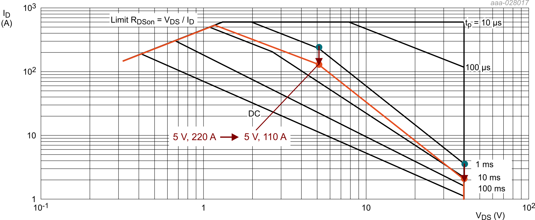
The complete Hot-SOA graph can be found by taking the following steps (current scaling method is used but this can be adapted to the other methods):
- The RDSon limit is not derated since it is calculated using RDSon at 175 °C
- Linear mode inflexion point and breakdown limit are shifted downwards, the new current limits are found using the power scale factor (in this case 0.5). A new inflexion point for the Spirito region is generated at half the current of the original one
- Finally, the lines can be extended to the endpoints using the same slope.
SOA: pulse shape conversion
In certain applications the power may not be a rectangular pulse, or the duration may be different from the set given in the SOA graph. In both cases a power shape conversion can be carried out and operation within SOA verified. This conversion is exact if the MOSFET is operating in ohmic mode or linear mode. However, it might be inaccurate for operation in the Spirito region.
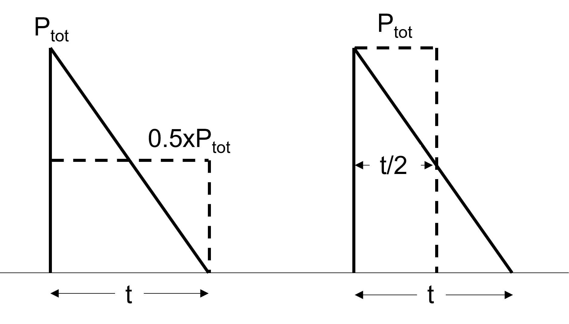
If the MOSFET is not working in Spirito region, the pulse can be converted into a rectangular one carrying the same amount of energy, by adjusting either the duration or the peak. Fig. 13 shows the conversion for a triangular power pulse. If the pulse duration is not part of the SOA graph, the limit can be calculated using the value of thermal impedance found in the data sheet (or an RC thermal model) and Equation 4. The use of thermal and electrothermal models is always recommended to accurately predict the junction temperature.
If the device is working in Spirito region, the pulse cannot be converted by means of the thermal impedance. In this case, the use of thermal and electrothermal models gives only an average junction temperature, which doesn’t reflect hot spots’ temperature. A conservative approach would be to consider a rectangular pulse with the same peak and duration of the original one. However, empirical evidence would suggest that triangular pulses can be converted into rectangular ones having same duration but half the peak value. Testing has been conducted using the BUK7S1R0-40H and the active clamp circuit shown in simulation 2. It is worth noting that these results should be considered valid only for this specific device.
Active clamping is used in inductive switching, similarly to avalanche, however the device operates in linear mode at a lower clamping voltage than in avalanche. With switch sw1 on the closed position and MOSFET M1 turned ON, current can flow through the main circuit. Once the inductor is “charged” the MOSFET is switched OFF. The energy stored in the inductor induces a high voltage that breaks down the Zener diode ZD1. This, in turn, clamps the gate voltage turning ON the MOSFET, which absorbs the energy released by the inductor. During this last activation the MOSFET is working in linear mode, the VDS is fairly constant while its drain current decreases, as shown in Fig. 14 (simulated). Therefore, the dissipated power is a triangular pulse lasting 1 ms.
Figure 15. Current versus time capability of avalanche and active clamp of BUK7S1R0-40H
The circuit is used to test the BUK7S1R0-40H at VDS of 20 V, 22 V and 28 V. The limit is obtained by derating the current at which destruction occurs by applying the same methodology used for the SOA in data sheets. Fig. 15 shows the current capability against time in avalanche (IAL) and during active clamp at different clamping voltages. Table 2 summarises the results from the graph at a pulse of 1 ms. The current capability for a triangular pulse is shown to be around 2x the one for a rectangular pulse. The current decreases as the voltage increases, as expected in case of rectangular pulses.
| Voltage | 1 ms active clamp current (A) |
1 ms SOA (data sheet) current (A) |
|---|---|---|
| 20 | 35 | 16 |
| 22 | 31 | 14 |
| 28 | 15 | 8 |
The same principle applies to capacitive pre-charge, where the MOSFET dissipates a triangular power pulse. However, in this case the ID is constant and VDS decreases. The reducing voltage leads the working point to move towards the left of the SOA graph away from the Spirito region, with lower risks of thermal instability with respect to active clamp.
Summary
In this interactive application note an overview of power MOSFETs linear mode operation has been presented. Together with embedded simulations a brief theoretical introduction highlighting the main differences with RDSon mode, the link between linear mode and SOA have been described. This includes thermal instability (Spirito region), Hot-SOA derating methods and pulse shape conversion.
Reference
1 Electro-thermal instability in low voltage power MOS: Experimental characterization - IEEE; G. Breglio, F. Frisina, A. Magri, P. Spirito
| Page last updated 09 May 2022. |