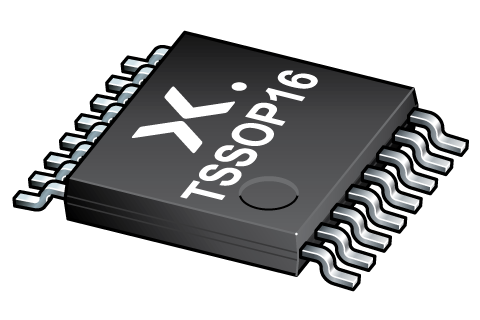
可訂購部件
| 型號(hào) | 可訂購的器件編號(hào) | 訂購代碼(12NC) | 封裝 | 從經(jīng)銷商處購買 |
|---|---|---|---|---|
| 74AVCH4T245PW | 74AVCH4T245PW,118 | 935284589118 | SOT403-1 | 訂單產(chǎn)品 |
進(jìn)一步了解Nexperia的豐富產(chǎn)品組合,比如二極管、雙極性晶體管、ESD保護(hù)器件、MOSFET器件、氮化鎵場(chǎng)效應(yīng)晶體管(GaN FET)、絕緣柵雙極晶體管(IGBT)以及模擬IC和邏輯IC。我們的器件廣泛應(yīng)用于汽車、工業(yè)、移動(dòng)和消費(fèi)等多個(gè)領(lǐng)域,幾乎為世界上所有電子設(shè)計(jì)提供支持。
我們的產(chǎn)品在各行各業(yè)均有應(yīng)用,包括汽車、工業(yè)、電力、計(jì)算、消費(fèi)、移動(dòng)和可穿戴設(shè)備等行業(yè)。憑借對(duì)創(chuàng)新和可持續(xù)發(fā)展的不懈承諾,我們的器件成為了行業(yè)效率基準(zhǔn),可幫助全球客戶群體開發(fā)高效節(jié)能的前沿解決方案。
試用我們種類齊全的評(píng)估板,體驗(yàn)我們的設(shè)備及其性能。深入了解我們的產(chǎn)品如何助您提高效率、穩(wěn)健性和可靠性,讓您的應(yīng)用大受裨益。您可以在這里找到聚焦在應(yīng)用、封裝和不同的 Nexperia 產(chǎn)品的評(píng)估板。

Register once, drag and drop ECAD models into your CAD tool and speed up your design.
Click here for more information4-bit dual supply translating transceiver with configurable voltage translation; 3-state
The 74AVCH4T245 is a 4-bit, dual supply transceiver that enables bidirectional level translation. The device can be used as two 2-bit transceivers or as a 4-bit transceiver. It features two 2-bit input-output ports (nAn and nBn), a direction control input (nDIR), an output enable input (nOE) and dual supply pins (VCC(A) and VCC(B)). Both VCC(A) and VCC(B) can be supplied at any voltage between 0.8 V and 3.6 V making the device suitable for translating between any of the low voltage nodes (0.8 V, 1.2 V, 1.5 V, 1.8 V, 2.5 V and 3.3 V). Pins nAn, nOE and nDIR are referenced to VCC(A) and pins nBn are referenced to VCC(B). A HIGH on nDIR allows transmission from nAn to nBn and a LOW on nDIR allows transmission from nBn to nAn. The output enable input (nOE) can be used to disable the outputs so the buses are effectively isolated.
The device is fully specified for partial power-down applications using IOFF. The IOFF circuitry disables the output, preventing any damaging backflow current through the device when it is powered down. In suspend mode when either VCC(A) or VCC(B) are at GND level, both nAn and nBn outputs are in the high-impedance OFF-state. The bus hold circuitry on the powered-up side always stays active.
The 74AVCH4T245 has active bus hold circuitry which is provided to hold unused or floating data inputs at a valid logic level. This feature eliminates the need for external pull-up or pull-down resistors.
Wide supply voltage range: VCC(A): 0.8 V to 3.6 V; VCC(B): 0.8 V to 3.6 V
Complies with JEDEC standards:
JESD8-12 (0.8 V to 1.3 V)
JESD8-11 (0.9 V to 1.65 V)
JESD8-7 (1.2 V to 1.95 V)
JESD8-5 (1.8 V to 2.7 V)
JESD8-B (2.7 V to 3.6 V)
Maximum data rates:
380 Mbit/s (≥ 1.8 V to 3.3 V translation)
200 Mbit/s (≥ 1.1 V to 3.3 V translation)
200 Mbit/s (≥ 1.1 V to 2.5 V translation)
200 Mbit/s (≥ 1.1 V to 1.8 V translation)
150 Mbit/s (≥ 1.1 V to 1.5 V translation)
100 Mbit/s (≥ 1.1 V to 1.2 V translation)
Suspend mode
Bus hold on data inputs
Latch-up performance exceeds 100 mA per JESD 78 Class II
Inputs accept voltages up to 3.6 V
IOFF circuitry provides partial Power-down mode operation
ESD protection:
HBM: ANSI/ESDA/JEDEC JS-001 class 3B exceeds 8000 V
CDM: ANSI/ESDA/JEDEC JS-002 class C3 exceeds 1000 V
Multiple package options
Specified from -40 °C to +85 °C and -40 °C to +125 °C
| 型號(hào) | VCC(A) (V) | VCC(B) (V) | Logic switching levels | Output drive capability (mA) | tpd (ns) | Nr of bits | Power dissipation considerations | Tamb (°C) | Rth(j-a) (K/W) | Ψth(j-top) (K/W) | Rth(j-c) (K/W) | Package name | Category |
|---|---|---|---|---|---|---|---|---|---|---|---|---|---|
| 74AVCH4T245PW | 0.8?-?3.6 | 0.8?-?3.6 | CMOS/LVTTL | ± 12 | 2.1 | 4 | very low | -40~125 | 124 | 4.4 | 53.6 | TSSOP16 | Bi-directional | Direction controlled |
| Model Name | 描述 |
|---|---|
|
|
| 型號(hào) | 可訂購的器件編號(hào),(訂購碼(12NC)) | 狀態(tài) | 標(biāo)示 | 封裝 | 外形圖 | 回流焊/波峰焊 | 包裝 |
|---|---|---|---|---|---|---|---|
| 74AVCH4T245PW | 74AVCH4T245PW,118 (935284589118) |
Active | CH4T245 |

TSSOP16 (SOT403-1) |
SOT403-1 |
SSOP-TSSOP-VSO-WAVE
|
SOT403-1_118 |
| 型號(hào) | 可訂購的器件編號(hào) | 化學(xué)成分 | RoHS | RHF指示符 |
|---|---|---|---|---|
| 74AVCH4T245PW | 74AVCH4T245PW,118 | 74AVCH4T245PW |
|
|
| 文件名稱 | 標(biāo)題 | 類型 | 日期 |
|---|---|---|---|
| 74AVCH4T245 | 4-bit dual supply translating transceiver with configurable voltage translation; 3-state | Data sheet | 2024-04-11 |
| AN90007 | Pin FMEA for AVC family | Application note | 2018-11-30 |
| Nexperia_document_guide_Logic_translators | Nexperia Logic Translators | Brochure | 2021-04-12 |
| SOT403-1 | 3D model for products with SOT403-1 package | Design support | 2020-01-22 |
| avch4t245 | 74AVCH4T245 IBIS model | IBIS model | 2019-01-09 |
| Nexperia_package_poster | Nexperia package poster | Leaflet | 2020-05-15 |
| TSSOP16_SOT403-1_mk | plastic, thin shrink small outline package; 16 leads; 0.65 mm pitch; 5 mm x 4.4 mm x 1.1 mm body | Marcom graphics | 2017-01-28 |
| SOT403-1 | plastic, thin shrink small outline package; 16 leads; 5 mm x 4.4 mm x 1.2 mm body | Package information | 2023-11-08 |
| SOT403-1_118 | TSSOP16; Reel pack for SMD, 13"; Q1/T1 product orientation | Packing information | 2020-04-21 |
| 74AVCH4T245PW_Nexperia_Product_Reliability | 74AVCH4T245PW Nexperia Product Reliability | Quality document | 2025-03-20 |
| SSOP-TSSOP-VSO-WAVE | Footprint for wave soldering | Wave soldering | 2009-10-08 |
The Nexperia Longevity Program is aimed to provide our customers information from time to time about the expected time that our products can be ordered. The NLP is reviewed and updated regularly by our Executive Management Team. View our longevity program here.
| Model Name | 描述 |
|---|---|
|
|
| 型號(hào) | Orderable part number | Ordering code (12NC) | 狀態(tài) | 包裝 | Packing Quantity | 在線購買 |
|---|---|---|---|---|---|---|
| 74AVCH4T245PW | 74AVCH4T245PW,118 | 935284589118 | Active | SOT403-1_118 | 2,500 | 訂單產(chǎn)品 |
作為 Nexperia 的客戶,您可以通過我們的銷售機(jī)構(gòu)訂購樣品。
如果您沒有 Nexperia 的直接賬戶,我們的全球和地區(qū)分銷商網(wǎng)絡(luò)可為您提供 Nexperia 樣品支持。查看官方經(jīng)銷商列表。
The interactive datasheets are based on the Nexperia MOSFET precision electrothermal models. With our interactive datasheets you can simply specify your own conditions interactively. Start by changing the values of the conditions. You can do this by using the sliders in the condition fields. By dragging the sliders you will see how the MOSFET will perform at the new conditions set.