Register once, drag and drop ECAD models into your CAD tool and speed up your design.
Click here for more information74HC194D
4-bit bidirectional universal shift register
The 74HC194 is a 4-bit bidirectional universal shift register. The synchronous operation of the device is determined by the mode select inputs (S0, S1). In parallel load mode (S0 and S1 HIGH) data appearing on the D0 to D3 inputs, when S0 and S1 are HIGH, is transferred to the Q0 to Q3 outputs. When S0 is HIGH and S1 is LOW data is entered serially via DSL and shifted from left to right; when S0 is LOW and S1 is HIGH data is entered serially via DSR and shifted from right to left. DSR and DSL allow multistage shift right or shift left data transfers without interfering with parallel load operation. If both S0 and S1 are LOW, existing data is retained in a hold mode. Mode select and data inputs are edge-triggered, responding only to the LOW-to-HIGH transition of the clock (CP). Therefore, the only timing restriction is that the mode control and selected data inputs must be stable one set-up time prior to the positive transition of the clock pulse. When LOW, the asynchronous master reset (MR) overrides all other input conditions and forces the Q outputs LOW. Inputs include clamp diodes. This enables the use of current limiting resistors to interface inputs to voltages in excess of VCC.
Features and benefits
Wide supply voltage range from 2.0 V to 6.0 V
CMOS low power dissipation
High noise immunity
Latch-up performance exceeds 100 mA per JESD 78 Class II Level B
Complies with JEDEC standards:
- JESD8C (2.7 V to 3.6 V)
- JESD7A (2.0 V to 6.0 V)
CMOS input levels
Shift-left and shift right capability
Synchronous parallel and serial data transfer
Easily expanded for both serial and parallel operation
Asynchronous master reset
Hold (‘do nothing’) mode
ESD protection:
HBM JESD22-A114F exceeds 2000 V
MM JESD22-A115-A exceeds 200 V
Specified from -40 °C to +85 °C and -40 °C to +125 °C
參數(shù)類型
| 型號(hào) | Package name |
|---|---|
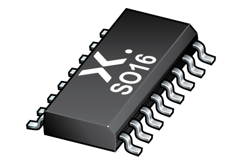
| 74HC194D | SO16 |
PCB Symbol, Footprint and 3D Model
| Model Name | 描述 |
|---|---|
|
|
封裝
下表中的所有產(chǎn)品型號(hào)均已停產(chǎn) 。
| 型號(hào) | 可訂購(gòu)的器件編號(hào),(訂購(gòu)碼(12NC)) | 狀態(tài) | 標(biāo)示 | 封裝 | 外形圖 | 回流焊/波峰焊 | 包裝 |
|---|---|---|---|---|---|---|---|
| 74HC194D | 74HC194D,652 (933714090652) |
Obsolete | 74HC194D |

SO16 (SOT109-1) |
SOT109-1 |
SO-SOJ-REFLOW
SO-SOJ-WAVE WAVE_BG-BD-1 |
SOT109-1_652 |
| 74HC194D,653 (933714090653) |
Obsolete | 74HC194D | 暫無(wú)信息 |
環(huán)境信息
下表中的所有產(chǎn)品型號(hào)均已停產(chǎn) 。
| 型號(hào) | 可訂購(gòu)的器件編號(hào) | 化學(xué)成分 | RoHS | RHF指示符 |
|---|---|---|---|---|
| 74HC194D | 74HC194D,652 | 74HC194D |
|
|
| 74HC194D | 74HC194D,653 | 74HC194D |
|
|
文檔 (11)
| 文件名稱 | 標(biāo)題 | 類型 | 日期 |
|---|---|---|---|
| 74HC194 | 4-bit bidirectional universal shift register | Data sheet | 2021-03-16 |
| AN11044 | Pin FMEA 74HC/74HCT family | Application note | 2019-01-09 |
| AN90063 | Questions about package outline drawings | Application note | 2025-03-12 |
| SOT109-1 | 3D model for products with SOT109-1 package | Design support | 2020-01-22 |
| Nexperia_package_poster | Nexperia package poster | Leaflet | 2020-05-15 |
| SO16_SOT109-1_mk | plastic, small outline package; 16 leads; 1.27 mm pitch; 9.9 mm x 3.9 mm x 1.35 mm body | Marcom graphics | 2017-01-28 |
| SOT109-1 | plastic, small outline package; 16 leads; 1.27 mm pitch; 9.9 mm x 3.9 mm x 1.75 mm body | Package information | 2023-11-07 |
| SO-SOJ-REFLOW | Footprint for reflow soldering | Reflow soldering | 2009-10-08 |
| HCT_USER_GUIDE | HC/T User Guide | User manual | 1997-10-31 |
| SO-SOJ-WAVE | Footprint for wave soldering | Wave soldering | 2009-10-08 |
| WAVE_BG-BD-1 | Wave soldering profile | Wave soldering | 2021-09-08 |
Longevity
The Nexperia Longevity Program is aimed to provide our customers information from time to time about the expected time that our products can be ordered. The NLP is reviewed and updated regularly by our Executive Management Team. View our longevity program here.
模型
| 文件名稱 | 標(biāo)題 | 類型 | 日期 |
|---|---|---|---|
| SOT109-1 | 3D model for products with SOT109-1 package | Design support | 2020-01-22 |
PCB Symbol, Footprint and 3D Model
| Model Name | 描述 |
|---|---|
|
|
How does it work?
The interactive datasheets are based on the Nexperia MOSFET precision electrothermal models. With our interactive datasheets you can simply specify your own conditions interactively. Start by changing the values of the conditions. You can do this by using the sliders in the condition fields. By dragging the sliders you will see how the MOSFET will perform at the new conditions set.