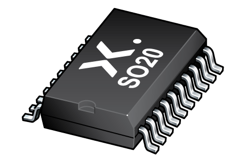
可訂購部件
| 型號 | 可訂購的器件編號 | 訂購代碼(12NC) | 封裝 | 從經銷商處購買 |
|---|---|---|---|---|
| 74HC299D | 74HC299D,653 | 933713540653 | SOT163-1 | 訂單產品 |

Register once, drag and drop ECAD models into your CAD tool and speed up your design.
Click here for more information8-bit universal shift register; 3-state
The 74HC299 is an 8?-?bit universal shift register with 3?-?state outputs. It contains eight edge?-?triggered D?-?type flip?-?flops and the interstage logic necessary to perform synchronous shift?-?right, shift?-?left, parallel load and hold operations. The type of operation is determined by the mode select inputs S0 and S1. Pins I/O0 to I/O7 are flip?-?flop 3?-?state buffer outputs which allow them to operate as data inputs in parallel load mode. The serial outputs Q0 and Q7 are used for expansion in serial shifting of longer words. A LOW signal on the asynchronous master reset input MR overrides the Sn and clock CP inputs and resets the flip?-?flops. All other state changes are initiated by the rising edge of the clock pulse. Inputs can change when the clock is either state, provided that the recommended set?-?up and hold times are observed. A HIGH signal on the 3?-?state output enable inputs OE1 or OE2 disables the 3?-?state buffers and the I/On outputs assume a high?-?impedance OFF?-?state. In this condition, the shift, hold, load and reset operations can still occur. The 3?-?state buffers are also disabled by HIGH signals on both S0 and S1, when in preparation for a parallel load operation. Inputs include clamp diodes. This enables the use of current limiting resistors to interface inputs to voltages in excess of VCC.
CMOS input levels
Multiplexed inputs/outputs provide improved bit density
Four operating modes:
Shift left
Shift right
Hold (store)
Load data
Operates with output enable or at high-impedance OFF-state
3-state outputs drive bus lines directly
Cascadable for n-bit word lengths
ESD protection:
HBM: ANSI/ESDA/JEDEC JS-001 class 2 exceeds 2000 V
CDM: ANSI/ESDA/JEDEC JS-002 class C3 exceeds 1000 V
Specified from -40 °C to +85 °C and from -40 °C to +125 °C
| 型號 | VCC (V) | Logic switching levels | Output drive capability (mA) | tpd (ns) | fmax (MHz) | Nr of bits | Power dissipation considerations | Tamb (°C) | Rth(j-a) (K/W) | Ψth(j-top) (K/W) | Rth(j-c) (K/W) | Package name |
|---|---|---|---|---|---|---|---|---|---|---|---|---|
| 74HC299D | 2.0?-?6.0 | CMOS | ± 7.8 | 19 | 54 | 8 | low | -40~125 | 63 | 6 | 38 | SO20 |
| Model Name | 描述 |
|---|---|
|
|
| 型號 | 可訂購的器件編號,(訂購碼(12NC)) | 狀態 | 標示 | 封裝 | 外形圖 | 回流焊/波峰焊 | 包裝 |
|---|---|---|---|---|---|---|---|
| 74HC299D | 74HC299D,653 (933713540653) |
Active | 74HC299D |

SO20 (SOT163-1) |
SOT163-1 |
WAVE_BG-BD-1
|
暫無信息 |
| 文件名稱 | 標題 | 類型 | 日期 |
|---|---|---|---|
| 74HC299 | 8-bit universal shift register; 3-state | Data sheet | 2024-08-05 |
| AN11044 | Pin FMEA 74HC/74HCT family | Application note | 2019-01-09 |
| AN90063 | Questions about package outline drawings | Application note | 2025-03-12 |
| SOT163-1 | 3D model for products with SOT163-1 package | Design support | 2020-01-22 |
| Nexperia_package_poster | Nexperia package poster | Leaflet | 2020-05-15 |
| SOT163-1 | plastic, small outline package; 20 leads; 1.27 mm pitch; 12.8 mm x 7.5 mm x 2.65 mm body | Package information | 2024-11-15 |
| 74HC299D_Nexperia_Product_Reliability | 74HC299D Nexperia Product Reliability | Quality document | 2025-03-20 |
| HCT_USER_GUIDE | HC/T User Guide | User manual | 1997-10-31 |
| WAVE_BG-BD-1 | Wave soldering profile | Wave soldering | 2021-09-08 |
The Nexperia Longevity Program is aimed to provide our customers information from time to time about the expected time that our products can be ordered. The NLP is reviewed and updated regularly by our Executive Management Team. View our longevity program here.
| 文件名稱 | 標題 | 類型 | 日期 |
|---|---|---|---|
| SOT163-1 | 3D model for products with SOT163-1 package | Design support | 2020-01-22 |
| Model Name | 描述 |
|---|---|
|
|
| 型號 | Orderable part number | Ordering code (12NC) | 狀態 | 包裝 | Packing Quantity | 在線購買 |
|---|---|---|---|---|---|---|
| 74HC299D | 74HC299D,653 | 933713540653 | Active | 暫無信息 | 2,000 | 訂單產品 |
作為 Nexperia 的客戶,您可以通過我們的銷售機構訂購樣品。
如果您沒有 Nexperia 的直接賬戶,我們的全球和地區分銷商網絡可為您提供 Nexperia 樣品支持。查看官方經銷商列表。
The interactive datasheets are based on the Nexperia MOSFET precision electrothermal models. With our interactive datasheets you can simply specify your own conditions interactively. Start by changing the values of the conditions. You can do this by using the sliders in the condition fields. By dragging the sliders you will see how the MOSFET will perform at the new conditions set.