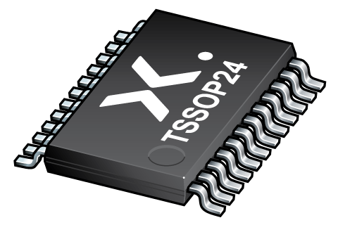
可訂購部件
| 型號 | 可訂購的器件編號 | 訂購代碼(12NC) | 封裝 | 從經銷商處購買 |
|---|---|---|---|---|
| 74HC4067PW-Q100 | 74HC4067PW-Q100J | 935306642118 | SOT355-1 | 訂單產品 |

Register once, drag and drop ECAD models into your CAD tool and speed up your design.
Click here for more information16-channel analog multiplexer/demultiplexer
The 74HC4067-Q100; 74HCT4067-Q100 is a single-pole 16-throw analog switch (SP16T) suitable for use in analog or digital 16:1 multiplexer/demultiplexer applications. The switch features four digital select inputs (S0, S1, S2 and S3), sixteen independent inputs/outputs (Yn), a common input/output (Z) and a digital enable input (E). When E is HIGH, the switches are turned off. Inputs include clamp diodes. This enables the use of current limiting resistors to interface inputs to voltages in excess of VCC.
This product has been qualified to the Automotive Electronics Council (AEC) standard Q100 (Grade 1) and is suitable for use in automotive applications.
Automotive product qualification in accordance with AEC-Q100 (Grade 1)
Specified from -40 °C to +85 °C and from -40 °C to +125 °C
Wide supply voltage range from 2.0 V to 10.0 V
Input levels S0, S1, S2, S3 and E inputs:
For 74HC4067-Q100: CMOS level
For 74HCT4067-Q100: TTL level
CMOS low power dissipation
High noise immunity
Typical ‘break before make’ built-in
Low ON resistance:
80 Ω (typical) at VCC = 4.5 V
70 Ω (typical) at VCC = 6.0 V
60 Ω (typical) at VCC = 9.0 V
Complies with JEDEC standards:
JESD8C (2.7 V to 3.6 V)
JESD7A (2.0 V to 6.0 V)
Latch-up performance exceeds 100 mA per JESD 78 Class II Level B
ESD protection:
HBM: ANSI/ESDA/JEDEC JS-001 class 2 exceeds 2000 V
CDM: ANSI/ESDA/JEDEC JS-002 class C3 exceeds 1000 V
Multiple package options
DHVQFN package with Side-Wettable Flanks enabling Automated Optical Inspection (AOI) of solder joints
Analog multiplexing and demultiplexing
Digital multiplexing and demultiplexing
Signal gating
| 型號 | Configuration | VCC (V) | RON (Ω) | Logic switching levels | Power dissipation considerations | Tamb (°C) | Rth(j-a) (K/W) | Ψth(j-top) (K/W) | Rth(j-c) (K/W) | Package name |
|---|---|---|---|---|---|---|---|---|---|---|
| 74HC4067PW-Q100 | SP16T-Z | 2.0?-?10.0 | 200 | CMOS | very low | -40~125 | 78 | 1.7 | 32 | TSSOP24 |
| Model Name | 描述 |
|---|---|
|
|
| 型號 | 可訂購的器件編號,(訂購碼(12NC)) | 狀態 | 標示 | 封裝 | 外形圖 | 回流焊/波峰焊 | 包裝 |
|---|---|---|---|---|---|---|---|
| 74HC4067PW-Q100 | 74HC4067PW-Q100J (935306642118) |
Active | HC4067 |

TSSOP24 (SOT355-1) |
SOT355-1 |
SSOP-TSSOP-VSO-WAVE
|
SOT355-1_118 |
| 文件名稱 | 標題 | 類型 | 日期 |
|---|---|---|---|
| 74HC_HCT4067_Q100 | 16-channel analog multiplexer/demultiplexer | Data sheet | 2024-07-25 |
| AN11044 | Pin FMEA 74HC/74HCT family | Application note | 2019-01-09 |
| SOT355-1 | 3D model for products with SOT355-1 package | Design support | 2020-01-22 |
| Nexperia_package_poster | Nexperia package poster | Leaflet | 2020-05-15 |
| SOT355-1 | plastic, thin shrink small outline package; 24 leads; 0.65 mm pitch; 7.8 mm x 4.4 mm x 1.2 mm body | Package information | 2024-11-15 |
| SOT355-1_118 | TSSOP24; Reel pack for SMD 13''; Q1/T1 product orientation | Packing information | 2020-04-21 |
| 74HC4067PW-Q100_Nexperia_Product_Reliability | 74HC4067PW-Q100 Nexperia Product Reliability | Quality document | 2025-03-20 |
| HCT_USER_GUIDE | HC/T User Guide | User manual | 1997-10-31 |
| SSOP-TSSOP-VSO-WAVE | Footprint for wave soldering | Wave soldering | 2009-10-08 |
The Nexperia Longevity Program is aimed to provide our customers information from time to time about the expected time that our products can be ordered. The NLP is reviewed and updated regularly by our Executive Management Team. View our longevity program here.
| 文件名稱 | 標題 | 類型 | 日期 |
|---|---|---|---|
| SOT355-1 | 3D model for products with SOT355-1 package | Design support | 2020-01-22 |
| Model Name | 描述 |
|---|---|
|
|
| 型號 | Orderable part number | Ordering code (12NC) | 狀態 | 包裝 | Packing Quantity | 在線購買 |
|---|---|---|---|---|---|---|
| 74HC4067PW-Q100 | 74HC4067PW-Q100J | 935306642118 | Active | SOT355-1_118 | 2,500 | 訂單產品 |
作為 Nexperia 的客戶,您可以通過我們的銷售機構訂購樣品。
如果您沒有 Nexperia 的直接賬戶,我們的全球和地區分銷商網絡可為您提供 Nexperia 樣品支持。查看官方經銷商列表。
The interactive datasheets are based on the Nexperia MOSFET precision electrothermal models. With our interactive datasheets you can simply specify your own conditions interactively. Start by changing the values of the conditions. You can do this by using the sliders in the condition fields. By dragging the sliders you will see how the MOSFET will perform at the new conditions set.