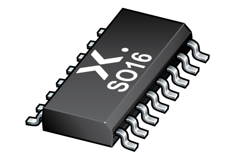
可訂購部件
| 型號 | 可訂購的器件編號 | 訂購代碼(12NC) | 封裝 | 從經銷商處購買 |
|---|---|---|---|---|
| 74HCT4851D-Q100 | 74HCT4851D-Q100,11 | 935298465118 | SOT109-1 | 訂單產品 |

Register once, drag and drop ECAD models into your CAD tool and speed up your design.
Click here for more information8-channel analog multiplexer/demultiplexer with injection?-?current effect control
The 74HC4851-Q100; 74HCT4851-Q100 are high-speed Si-gate CMOS devices and are specified in compliance with JEDEC standard no. 7A.
The 74HC4851-Q100; 74HCT4851-Q100 are 8-channel analog multiplexers/demultiplexers with three digital select inputs (S0 to S2), an active-LOW enable input (E), eight independent inputs?/?outputs (Y0 to Y7) and a common input/output (Z). The devices feature injection-current effect control, which has excellent value in automotive applications where voltages in excess of the supply voltage are common.
With E LOW, one of the eight switches is selected (low impedance ON-state) by S0 to S2. With E HIGH, all switches are in the high-impedance OFF-state, independent of S0 to S2.
The injection-current effect control allows signals at disabled analog input channels to exceed the supply voltage without affecting the signal of the enabled analog channel. This eliminates the need for external diode/resistor networks typically used to keep the analog channel signals within the supply-voltage range.
This product has been qualified to the Automotive Electronics Council (AEC) standard Q100 (Grade 1) and is suitable for use in automotive applications.
Automotive product qualification in accordance with AEC-Q100 (Grade 1)
Specified from -40 °C to +85 °C and from -40 °C to +125 °C
Injection-current cross coupling < 1 mV/mA
Wide supply voltage range from 2.0 V to 6.0 V for 74HC4851-Q100
Latch-up performance exceeds 100 mA per JESD 78 Class II level A
Low ON-state resistance:
400 Ω (typical) at VCC = 2.0 V
215 Ω (typical) at VCC = 3.0 V
120 Ω (typical) at VCC = 3.3 V
76 Ω (typical) at VCC = 4.5 V
59 Ω (typical) at VCC = 6.0 V
ESD protection:
HBM: ANSI/ESDA/JEDEC JS-001 class 2 exceeds 2000 V
CDM: ANSI/ESDA/JEDEC JS-002 class C3 exceeds 1000 V
Multiple package options
DHVQFN package with Side-Wettable Flanks enabling Automatic Optical Inspection (AOI) of solder joints
Analog multiplexing and demultiplexing
Digital multiplexing and demultiplexing
Signal gating
Automotive application
| 型號 | Configuration | VCC (V) | RON (Ω) | Logic switching levels | Power dissipation considerations | Tamb (°C) | Rth(j-a) (K/W) | Ψth(j-top) (K/W) | Rth(j-c) (K/W) | Package name |
|---|---|---|---|---|---|---|---|---|---|---|
| 74HCT4851D-Q100 | SP8T-Z | 4.5?-?5.5 | 240 | TTL | very low | -40~125 | 79 | 3.8 | 37.7 | SO16 |
| Model Name | 描述 |
|---|---|
|
|
| 型號 | 可訂購的器件編號,(訂購碼(12NC)) | 狀態 | 標示 | 封裝 | 外形圖 | 回流焊/波峰焊 | 包裝 |
|---|---|---|---|---|---|---|---|
| 74HCT4851D-Q100 | 74HCT4851D-Q100,11 (935298465118) |
Active | 74HCT4851D |

SO16 (SOT109-1) |
SOT109-1 |
SO-SOJ-REFLOW
SO-SOJ-WAVE WAVE_BG-BD-1 |
SOT109-1_118 |
| 文件名稱 | 標題 | 類型 | 日期 |
|---|---|---|---|
| 74HC_HCT4851_Q100 | 8-channel analog multiplexer/demultiplexer with injection?-?current effect control | Data sheet | 2024-05-30 |
| AN11044 | Pin FMEA 74HC/74HCT family | Application note | 2019-01-09 |
| AN90063 | Questions about package outline drawings | Application note | 2025-03-12 |
| SOT109-1 | 3D model for products with SOT109-1 package | Design support | 2020-01-22 |
| Nexperia_package_poster | Nexperia package poster | Leaflet | 2020-05-15 |
| SO16_SOT109-1_mk | plastic, small outline package; 16 leads; 1.27 mm pitch; 9.9 mm x 3.9 mm x 1.35 mm body | Marcom graphics | 2017-01-28 |
| SOT109-1 | plastic, small outline package; 16 leads; 1.27 mm pitch; 9.9 mm x 3.9 mm x 1.75 mm body | Package information | 2023-11-07 |
| SOT109-1_118 | SO16; Reel pack for SMD, 13"; Q1/T1 product orientation | Packing information | 2024-02-19 |
| 74HCT4851D-Q100_Nexperia_Product_Reliability | 74HCT4851D-Q100 Nexperia Product Reliability | Quality document | 2025-03-20 |
| SO-SOJ-REFLOW | Footprint for reflow soldering | Reflow soldering | 2009-10-08 |
| HCT_USER_GUIDE | HC/T User Guide | User manual | 1997-10-31 |
| SO-SOJ-WAVE | Footprint for wave soldering | Wave soldering | 2009-10-08 |
| WAVE_BG-BD-1 | Wave soldering profile | Wave soldering | 2021-09-08 |
The Nexperia Longevity Program is aimed to provide our customers information from time to time about the expected time that our products can be ordered. The NLP is reviewed and updated regularly by our Executive Management Team. View our longevity program here.
| 文件名稱 | 標題 | 類型 | 日期 |
|---|---|---|---|
| SOT109-1 | 3D model for products with SOT109-1 package | Design support | 2020-01-22 |
| Model Name | 描述 |
|---|---|
|
|
| 型號 | Orderable part number | Ordering code (12NC) | 狀態 | 包裝 | Packing Quantity | 在線購買 |
|---|---|---|---|---|---|---|
| 74HCT4851D-Q100 | 74HCT4851D-Q100,11 | 935298465118 | Active | SOT109-1_118 | 2,500 | 訂單產品 |
作為 Nexperia 的客戶,您可以通過我們的銷售機構訂購樣品。
如果您沒有 Nexperia 的直接賬戶,我們的全球和地區分銷商網絡可為您提供 Nexperia 樣品支持。查看官方經銷商列表。
The interactive datasheets are based on the Nexperia MOSFET precision electrothermal models. With our interactive datasheets you can simply specify your own conditions interactively. Start by changing the values of the conditions. You can do this by using the sliders in the condition fields. By dragging the sliders you will see how the MOSFET will perform at the new conditions set.