Register once, drag and drop ECAD models into your CAD tool and speed up your design.
Click here for more information74LVC1G53GD
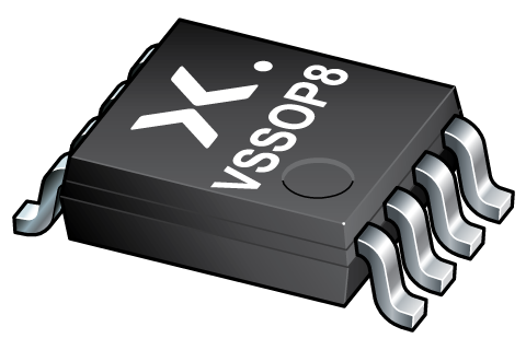
2-channel analog multiplexer/demultiplexer
The 74LVC1G53 is a single-pole double-throw analog switch with a digital select input (S), two independent inputs/outputs (Y0 and Y1), a common input/output (Z) and a digital enable input (E). When E is HIGH, the switch is turned off. Control inputs can be driven from either 3.3 V or 5 V devices. This feature allows the use of these devices as translators in mixed 3.3 V and 5 V environments.
Schmitt-trigger action at control inputs makes the circuit tolerant of slower input rise and fall times.
Alternatives
Features and benefits
Wide supply voltage range from 1.65 V to 5.5 V
Very low ON resistance:
7.5 Ω (typical) at VCC = 2.7 V
6.5 Ω (typical) at VCC = 3.3 V
6 Ω (typical) at VCC = 5 V
Switch current capability of 32 mA
High noise immunity
CMOS low power consumption
TTL interface compatibility at 3.3 V
Latch-up performance meets requirements of JESD 78 Class I
Control inputs accept voltages up to 5 V
ESD protection:
HBM: ANSI/ESDA/JEDEC JS-001 class 2 exceeds 2000 V
CDM: ANSI/ESDA/JEDEC JS-002 class C3 exceeds 1000 V
Multiple package options
Specified from -40 °C to +85 °C and from -40 °C to +125 °C
Longevity
The Nexperia Longevity Program is aimed to provide our customers information from time to time about the expected time that our products can be ordered. The NLP is reviewed and updated regularly by our Executive Management Team. View our longevity program here.
模型
| 文件名稱 | 標題 | 類型 | 日期 |
|---|---|---|---|
| lvc1g53 | 74LVC1G53 IBIS model | IBIS model | 2015-02-19 |
How does it work?
The interactive datasheets are based on the Nexperia MOSFET precision electrothermal models. With our interactive datasheets you can simply specify your own conditions interactively. Start by changing the values of the conditions. You can do this by using the sliders in the condition fields. By dragging the sliders you will see how the MOSFET will perform at the new conditions set.
