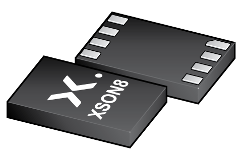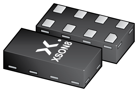
Register once, drag and drop ECAD models into your CAD tool and speed up your design.
Click here for more information74LVC1G99GD
Ultra-configurable multiple function gate; 3-state
The 74LVC1G99 provides a low voltage, ultra-configurable, multiple function gate with 3-state output. The device can be configured as one of several logic functions including, AND, OR, NAND, NOR, XOR, XNOR, inverter, buffer and MUX. No external components are required to configure the device as all inputs can be connected directly to VCC or GND. The 3-state output is controlled by the output enable input (OE). A HIGH level at OE causes the output (Y) to assume a high?-?impedance OFF-state. When OE is LOW, the output state is determined by the signals applied to the Schmitt trigger inputs (A, B, C and D).
Due to the use of Schmitt trigger inputs the device is tolerant of slowly changing input signals, transforming them into sharply defined, jitter free output signals. By eliminating leakage current paths to VCC and GND, the inputs and disabled output are also over-voltage tolerant, making the device suitable for mixed-voltage applications.
This device is fully specified for partial power-down applications using IOFF. The IOFF circuitry disables the output, preventing the damaging backflow current through the device when it is powered down.
The 74LVC1G99 is fully specified over the supply range from 1.65 V to 5.5 V.
Alternatives
Features and benefits
Wide supply voltage range from 1.65 V to 5.5 V
5 V tolerant inputs for interfacing with 5 V logic
High noise immunity
±24 mA output drive (VCC = 3.0 V)
CMOS low power consumption
Latch-up performance exceeds 250 mA
Direct interface with TTL levels
Inputs accept voltages up to 5 V
Complies with JEDEC standard:
JESD8-7 (1.65 V to 1.95 V)
JESD8-5 (2.3 V to 2.7 V)
JESD8-B/JESD36 (2.7 V to 3.6 V)
ESD protection:
HBM: ANSI/ESDA/JEDEC JS-001 class 2 exceeds 2000 V
CDM: ANSI/ESDA/JEDEC JS-002 class C3 exceeds 1000 V
Multiple package options
Specified from -40 °C to +85 °C and -40 °C to +125 °C.
參數類型
| 型號 | Package name |
|---|---|
| 74LVC1G99GD | XSON8 |
封裝
下表中的所有產品型號均已停產 。
| 型號 | 可訂購的器件編號,(訂購碼(12NC)) | 狀態 | 標示 | 封裝 | 外形圖 | 回流焊/波峰焊 | 包裝 |
|---|---|---|---|---|---|---|---|
| 74LVC1G99GD | 74LVC1G99GD,125 (935291883125) |
Obsolete | V99 Standard Procedure Standard Procedure |

XSON8 (SOT996-2) |
SOT996-2 | SOT996-2_125 |
Series
文檔 (5)
| 文件名稱 | 標題 | 類型 | 日期 |
|---|---|---|---|
| 74LVC1G99 | Ultra-configurable multiple function gate; 3-state | Data sheet | 2024-08-12 |
| AN11009 | Pin FMEA for LVC family | Application note | 2019-01-09 |
| lvc1g99 | 74LVC1G99 IBIS model | IBIS model | 2014-10-20 |
| Nexperia_package_poster | Nexperia package poster | Leaflet | 2020-05-15 |
| SOT996-2 | plastic, leadless extremely thin small outline package; 8 terminals; 0.5 mm pitch; 3 mm x 2 mm x 0.5 mm body | Package information | 2020-04-21 |
Longevity
The Nexperia Longevity Program is aimed to provide our customers information from time to time about the expected time that our products can be ordered. The NLP is reviewed and updated regularly by our Executive Management Team. View our longevity program here.
模型
| 文件名稱 | 標題 | 類型 | 日期 |
|---|---|---|---|
| lvc1g99 | 74LVC1G99 IBIS model | IBIS model | 2014-10-20 |
How does it work?
The interactive datasheets are based on the Nexperia MOSFET precision electrothermal models. With our interactive datasheets you can simply specify your own conditions interactively. Start by changing the values of the conditions. You can do this by using the sliders in the condition fields. By dragging the sliders you will see how the MOSFET will perform at the new conditions set.
