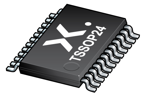
Register once, drag and drop ECAD models into your CAD tool and speed up your design.
Click here for more information74LVC827APW
10-bit buffer/line driver with 5 V tolerant inputs/outputs; 3-state
The 74LVC827A is a 10-bit buffer/line driver with 3-state outputs. The 3-state outputs are controlled by the output enable pins OE1 and OE2. A HIGH on pin OEn causes the outputs to assume a high-impedance OFF-state.
Inputs can be driven from either 3.3 V or 5 V devices. When disabled, up to 5.5 V can be applied to the outputs. These features allow the use of these devices as translators in mixed 3.3 V and 5 V applications.
Features and benefits
5 V tolerant inputs/outputs for interfacing with 5 V logic
Wide supply voltage range from 1.2 V to 3.6 V
CMOS low power consumption
Direct interface with TTL levels
Complies with JEDEC standard:
JESD8-7A (1.65 V to 1.95 V)
JESD8-5A (2.3 V to 2.7 V)
JESD8-C/JESD36 (2.7 V to 3.6 V)
ESD protection:
HBM EIA/JESD22-A114-F exceeds 2000 V
MM EIA/JESD22-A115-B exceeds 200 V
CDM JESD22-C101E exceeds 1000 V
Specified from -40 °C to +85 °C and -40 °C to +125 °C
Applications
參數類型
| 型號 | Package name |
|---|---|
| 74LVC827APW | TSSOP24 |
PCB Symbol, Footprint and 3D Model
| Model Name | 描述 |
|---|---|
|
|
封裝
下表中的所有產品型號均已停產 。
| 型號 | 可訂購的器件編號,(訂購碼(12NC)) | 狀態 | 標示 | 封裝 | 外形圖 | 回流焊/波峰焊 | 包裝 |
|---|---|---|---|---|---|---|---|
| 74LVC827APW | 74LVC827APW,112 (935262420112) |
Obsolete | LVC827A |

TSSOP24 (SOT355-1) |
SOT355-1 |
SSOP-TSSOP-VSO-WAVE
|
暫無信息 |
| 74LVC827APW,118 (935262420118) |
Obsolete | LVC827A | SOT355-1_118 |
環境信息
下表中的所有產品型號均已停產 。
| 型號 | 可訂購的器件編號 | 化學成分 | RoHS | RHF指示符 |
|---|---|---|---|---|
| 74LVC827APW | 74LVC827APW,112 | 74LVC827APW |
|
|
| 74LVC827APW | 74LVC827APW,118 | 74LVC827APW |
|
|
文檔 (9)
| 文件名稱 | 標題 | 類型 | 日期 |
|---|---|---|---|
| 74LVC827A | 10-bit buffer/line driver with 5 V tolerant inputs/outputs; 3-state | Data sheet | 2017-07-20 |
| AN11009 | Pin FMEA for LVC family | Application note | 2019-01-09 |
| AN263 | Power considerations when using CMOS and BiCMOS logic devices | Application note | 2023-02-07 |
| SOT355-1 | 3D model for products with SOT355-1 package | Design support | 2020-01-22 |
| lvc827a | lvc827a IBIS model | IBIS model | 2013-04-09 |
| Nexperia_package_poster | Nexperia package poster | Leaflet | 2020-05-15 |
| SOT355-1 | plastic, thin shrink small outline package; 24 leads; 0.65 mm pitch; 7.8 mm x 4.4 mm x 1.2 mm body | Package information | 2024-11-15 |
| lvc | lvc Spice model | SPICE model | 2013-05-07 |
| SSOP-TSSOP-VSO-WAVE | Footprint for wave soldering | Wave soldering | 2009-10-08 |
Longevity
The Nexperia Longevity Program is aimed to provide our customers information from time to time about the expected time that our products can be ordered. The NLP is reviewed and updated regularly by our Executive Management Team. View our longevity program here.
PCB Symbol, Footprint and 3D Model
| Model Name | 描述 |
|---|---|
|
|
How does it work?
The interactive datasheets are based on the Nexperia MOSFET precision electrothermal models. With our interactive datasheets you can simply specify your own conditions interactively. Start by changing the values of the conditions. You can do this by using the sliders in the condition fields. By dragging the sliders you will see how the MOSFET will perform at the new conditions set.