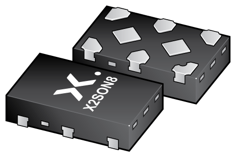
可訂購部件
| 型號 | 可訂購的器件編號 | 訂購代碼(12NC) | 封裝 | 從經銷商處購買 |
|---|---|---|---|---|
| NCA9306GX | NCA9306GXX | 935691025115 | SOT1233-2 | 訂單產品 |

Register once, drag and drop ECAD models into your CAD tool and speed up your design.
Click here for more information2-bit bidirectional multi-voltage level translator; open-drain; push-pull
The NCA9306 is a 2 channel bidirectional I2C and SMBus multi-voltage level translator with an enable (EN) pin input. It allows voltage translation between 0.95 V and 5 V without the use of a direction pin. It supports up to 100 MHz up translation and >100 MHz down translation at ≤ 30 pF capacitive load. There is no need for a direction pin which minimizes the system effort. The NCA9306 supports 5 V tolerant I/O pins to support mixed mode signal operation. The ability to set up different voltage translation levels on each channel makes the device very flexible and suitable for a lot of different applications.
The low ON-state resistance RON of the switch allows connections to be made with minimal propagation delay. When EN is HIGH, the translator switch is on, and the SCLA and SDAA I/O are connected to the SCLB and SDAB I/O respectively, allowing bidirectional data flow between ports. When EN is LOW, the translator switch is off, and a high-impedance state exists between ports. As with the standard I2C bus-system, pull-up resistors are required to provide the logic HIGH levels on the translators bus. The NCA9306 has a standard open-drain configuration of the I2C-bus. The size of these pull-up resistors depend on the system. Each side of the translator must have a pull?-?up resistors. NCA9306 is designed to work with Standard-mode, Fast-mode and Fast?-?mode plus I2C bus devices in addition to the SMBus devices.
When the SDAA or SDAB pin is LOW, the clamp is in the ON-state and a low resistance connections exists between the SDAA and SDAB ports. Assuming the higher voltage is on the SDAB port when the SDAB port is HIGH, the voltage on the SDAA port is limited to the voltage set by refA. When the SDAA port is HIGH, the SDAB port is pulled to the refB supply voltage by the pull-up resistors. The SCLA or SCLB pins also follows the same behavior as described for SDAA or SDAB pins.
2-channel bidirectional voltage translator for SDA and SCL lines in mixed mode I2C bus applications
Open-drain I2C-bus I/O ports (SCLA, SDAA, SCLB and SDAB)
Provides bidirectional voltage translation with no direction pin
High-impedance SCLA, SDAA, SCLB and SDAB for EN = LOW
Up translation
< 100 MHz; CL = 30 pF
< 40 MHz; CL = 50 pF
Down translation
> 100 MHz; CL = 30 pF
< 40 MHz; CL = 50 pF
Hot insertion
Bidirectional voltage level translation between:
0.95 V and 1.8 V, 2.5 V, 3.3 V and 5.0 V
1.2 V and 1.8 V, 2.5 V, 3.3 V and 5.0 V
1.8 V and 2.5 V, 3.3 V and 5.0 V
2.5 V and 3.3 V and 5.0 V
3.3 V and 5.0 V
Low standby current
5 V tolerant I2C-bus I/O pins to support mixed mode signal operation
Low RON provides less signal distortion
Latch-up performance exceeds 100 mA per JESD78 class II level A
ESD protection:
HBM ANSI/ESDA/JEDEC JS-001 class 2 exceeds 2000 V
CDM ANSI/ESDA/JEDEC JS-002 class C3 exceeds 1000 V
Specified from -40 °C to +125 °C
GPIO, MDIO, PMBus, SMBus, SDIO, UART, I2C, and other interfaces in Telecom infrastructure
Industrial
Personal computing
Router and Industrial Automation
| 型號 | VCC(A) (V) | VCC(B) (V) | Logic switching levels | Output drive capability (mA) | tpd (ns) | Nr of bits | Power dissipation considerations | Tamb (°C) | Rth(j-a) (K/W) | Ψth(j-top) (K/W) | Rth(j-c) (K/W) | Package name | Category |
|---|---|---|---|---|---|---|---|---|---|---|---|---|---|
| NCA9306GX | 0.95?-?5.0 | 0.95?-?5.0 | CMOS | + 64 | 0.4 | 2 | low | -40~125 | 407 | 7.9 | 200 | X2SON8 | Application specific |
| 型號 | 可訂購的器件編號,(訂購碼(12NC)) | 狀態 | 標示 | 封裝 | 外形圖 | 回流焊/波峰焊 | 包裝 |
|---|---|---|---|---|---|---|---|
| NCA9306GX | NCA9306GXX (935691025115) |
Active | h9 |

X2SON8 (SOT1233-2) |
SOT1233-2 | SOT1233-2_115 |
| 文件名稱 | 標題 | 類型 | 日期 |
|---|---|---|---|
| NCA9306 | 2-bit bidirectional multi-voltage level translator; open-drain; push-pull | Data sheet | 2024-08-05 |
| AN90033 | Bidirectional multi-voltage level translator applications using Nexperia's LSF010x auto-sense devices | Application note | 2022-09-02 |
| SOT1233-2 | 3D model for products with SOT1233-2 package | Design support | 2021-01-28 |
| nca9306 | NCA9306 IBIS model | IBIS model | 2020-09-23 |
| SOT1233-2 | plastic thermal enhanced extremely thin small outline package; no leads;8 terminals; body 1.35 x 0.8 x 0.32 mm | Package information | 2022-04-21 |
| SOT1233-2_115 | X2SON8; Reel pack for SMD, 7''; Q1/T1 product orientation | Packing information | 2020-05-12 |
| NCA9306GX_Nexperia_Product_Reliability | NCA9306GX Nexperia Product Reliability | Quality document | 2025-03-20 |
The Nexperia Longevity Program is aimed to provide our customers information from time to time about the expected time that our products can be ordered. The NLP is reviewed and updated regularly by our Executive Management Team. View our longevity program here.
| 型號 | Orderable part number | Ordering code (12NC) | 狀態 | 包裝 | Packing Quantity | 在線購買 |
|---|---|---|---|---|---|---|
| NCA9306GX | NCA9306GXX | 935691025115 | Active | SOT1233-2_115 | 10,000 | 訂單產品 |
作為 Nexperia 的客戶,您可以通過我們的銷售機構訂購樣品。
如果您沒有 Nexperia 的直接賬戶,我們的全球和地區分銷商網絡可為您提供 Nexperia 樣品支持。查看官方經銷商列表。
The interactive datasheets are based on the Nexperia MOSFET precision electrothermal models. With our interactive datasheets you can simply specify your own conditions interactively. Start by changing the values of the conditions. You can do this by using the sliders in the condition fields. By dragging the sliders you will see how the MOSFET will perform at the new conditions set.