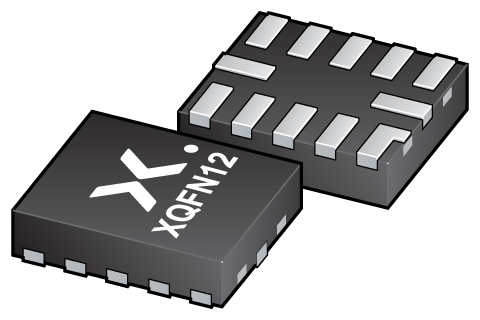
可訂購部件
| 型號 | 可訂購的器件編號 | 訂購代碼(12NC) | 封裝 | 從經銷商處購買 |
|---|---|---|---|---|
| NXU0204GU12-Q100 | NXU0204GU12-Q100X | 935691861115 | SOT1174-1 | 訂單產品 |

Register once, drag and drop ECAD models into your CAD tool and speed up your design.
Click here for more information4-bit dual-supply voltage level translating buffer with Schmitt-trigger; 3-state
The NXU0204-Q100 is a 4-bit, dual-supply level translating buffer with Schmitt-trigger inputs and 3-state outputs. It features four data inputs (A1, A2, B3 and B4), four data outputs (YB1, YB2, YA3 and YA4) and an output enable input (OE).
Both VCCA and VCCB can be supplied at any voltage between 0.9 V and 5.5 V making the device suitable for translating between any of the voltage nodes (1.2 V, 1.5 V, 1.8 V, 2.5 V, 3.3 V and 5.0 V).
This device facilitates asynchronous communication between data buses. Transmit data with a fixed direction (unidirectionally) from the A bus to the B bus on three channels and from the B bus to the A bus for on one channel. The OE pin can be referenced to VCCA and VCCB domain and when OE pin is set LOW the outputs are disabled and enter a high-impedance OFF?-?state which isolates the buses. The OE pin can be left floating or externally pulled down to ground to ensure the high-impedance state of the outputs during power up or power down.
This device ensures low static and dynamic power consumption across the entire supply range and is fully specified for partial power down applications using IOFF. The IOFF circuitry prevents potentially damaging backflow current through the device when it is powered down or if one of the power supplies is disconnected (floating).
No power supply sequencing is required and output glitches during power supply transitions are prevented. As a result, glitches will not appear on the outputs for supply transitions during power-up/down.
This product has been qualified to the Automotive Electronics Council (AEC) standard Q100 (Grade 1) and is suitable for use in automotive applications.
 |
Automotive product qualification in accordance with AEC-Q100 (Grade 1)
Specified from -40 °C to +85 °C and from -40 °C to +125 °C
Wide supply voltage range:
VCCA: 0.9 V to 5.5 V
VCCB: 0.9 V to 5.5 V
Maximum data rates:
250 Mbps (≥ 1.8 V to 5 V translation)
High output drive 12 mA at 5 V
Output enable (OE) allows connection to VCCA or VCCB domain
Suspend mode when either one of the supply voltages is below 100 mV or disconnected (floating)
Low noise overshoot and undershoot <10% of VCCO
IOFF circuitry provides partial power-down mode operation
Latch-up performance exceeds 100 mA per JESD78D Class II
Complies with JEDEC standard:
JESD8-12 (0.9 V to 1.3 V)
JESD8-11 (1.4 V to 1.6 V)
JESD8-7 (1.65 V to 1.95 V)
JESD8-5 (2.3 V to 2.7 V)
JESD8C (2.7 V to 3.6 V)
JESD12-6 (4.5 V to 5.5 V)
ESD protection:
HBM: ANSI/ESDA/JEDEC JS-001 class 2 exceeds 2500 V
CDM: ANSI/ESDA/JEDEC JS-002 class C3 exceeds 1500 V
Similar functions: NXU0104-Q100 and NXU0304-Q100
DHVQFN package with Side-Wettable Flanks enabling Automated Optical Inspection (AOI) of solder joints
| 型號 | VCC(A) (V) | VCC(B) (V) | Logic switching levels | Output drive capability (mA) | tpd (ns) | Nr of bits | Power dissipation considerations | Tamb (°C) | Rth(j-a) (K/W) | Ψth(j-top) (K/W) | Rth(j-c) (K/W) | Package name |
|---|---|---|---|---|---|---|---|---|---|---|---|---|
| NXU0204GU12-Q100 | 0.9?-?5.5 | 0.9?-?5.5 | CMOS/LVTTL | ± 12 | 8.1 | 4 | ultra low | -40~125 | 172 | 3.3 | 82 | XQFN12 |
| 型號 | 可訂購的器件編號,(訂購碼(12NC)) | 狀態 | 標示 | 封裝 | 外形圖 | 回流焊/波峰焊 | 包裝 |
|---|---|---|---|---|---|---|---|
| NXU0204GU12-Q100 | NXU0204GU12-Q100X (935691861115) |
Active | L5 |

XQFN12 (SOT1174-1) |
SOT1174-1 | SOT1174-1_115 |
| Part number | Description | Type | Quick links | Shop link |
|---|---|---|---|---|
|
描述 This NEVB-NXU0204 evaluation board is designed to evaluate the product performance and behavior of Nexperia NXU0104. The board simulates the device being used in a system by incorporating series resistors and parallel loads on each input/output line. Output enable (OE) is selected with a jumper to pull up to either VCCA or VCCB supply rail and each input has a Schmitt trigger to accommodate slow or noisy input signals with a weak 6.5 M? pull-down accommodates floating input signals.
|
類型 Evaluation board
|
Quick links
|
Shop link
|
| 文件名稱 | 標題 | 類型 | 日期 |
|---|---|---|---|
| NXU0204_Q100 | 4-bit dual-supply voltage level translating buffer with Schmitt-trigger; 3-state | Data sheet | 2024-12-02 |
| AN90057 | Pin FMEA for NXU family | Application note | 2024-09-11 |
| SOT1174-1 | 3D model for products with SOT1174-1 package | Design support | 2021-01-28 |
| nxu0204 | NXU0204 IBIS model | IBIS model | 2024-09-03 |
| enhanced_unidirectional_direction_translator_portfolio_leaflet | Enhanced Unidirectional Direction Translator Portfolio | Leaflet | 2024-12-11 |
| Nexperia_package_poster | Nexperia package poster | Leaflet | 2020-05-15 |
| SOT1174-1 | plastic, leadless extremely thin quad flat package; 12 terminals; 0.4 mm pitch; 2 mm x 1.7 mm x 0.5 mm body | Package information | 2024-04-11 |
| SOT1174-1_115 | XQFN12; Reel pack for SMD, 7''; Q1/T1 product orientation | Packing information | 2020-04-21 |
| NXU0204GU12-Q100_Nexperia_Product_Reliability | NXU0204GU12-Q100 Nexperia Product Reliability | Quality document | 2025-03-20 |
| UM90041 | NXU0104, NXU0204 and NXU0304 evaluation board | User manual | 2024-09-11 |
The Nexperia Longevity Program is aimed to provide our customers information from time to time about the expected time that our products can be ordered. The NLP is reviewed and updated regularly by our Executive Management Team. View our longevity program here.
| 型號 | Orderable part number | Ordering code (12NC) | 狀態 | 包裝 | Packing Quantity | 在線購買 |
|---|---|---|---|---|---|---|
| NXU0204GU12-Q100 | NXU0204GU12-Q100X | 935691861115 | Active | SOT1174-1_115 | 4,000 | 訂單產品 |
作為 Nexperia 的客戶,您可以通過我們的銷售機構訂購樣品。
如果您沒有 Nexperia 的直接賬戶,我們的全球和地區分銷商網絡可為您提供 Nexperia 樣品支持。查看官方經銷商列表。
The interactive datasheets are based on the Nexperia MOSFET precision electrothermal models. With our interactive datasheets you can simply specify your own conditions interactively. Start by changing the values of the conditions. You can do this by using the sliders in the condition fields. By dragging the sliders you will see how the MOSFET will perform at the new conditions set.