Register once, drag and drop ECAD models into your CAD tool and speed up your design.
Click here for more informationNPS1000UP
0.5 V to 1.0 V, 1.5 A peak, 11 mΩ, load switch
NPS1000 is a low voltage, single-channel load switch with a low RDS,ON (11 mΩ) to minimize IR drop and power loss. It supports up to 0.6 A RMS current and a peak current of 1.5 A.
The switch is controlled by an EN input which is compatible with 1.2 V logic levels. When the load switch is enabled, the internal switch charges the output capacitor with a controlled inrush current. When the switch is disabled, an 8 Ω on-chip resistor discharges the output to ground and keeps it from floating.
The IC is powered from a separate BIAS pin which is rated for 2.3 V to 5.0 V operation.
NPS1000 has an over-temperature protection that latches the device OFF when the internal junction temperature is above the set point (Tth(OTLO)). At this time, the internal switch is turned off and the output discharge element turns on to discharge the output capacitor. The load switch can be enabled again by toggling the EN pin.
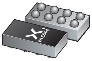
NPS1000 is available in an ultra-small, space saving, wafer level chip-scale package; 8 bumps; 1.42 mm × 0.72 mm × 0.465 mm body and is characterized for operation over junction temperature range of –?40 °C to 105 °C.
 |
Features and benefits
- 0.5 V – 1.0 V operation voltage
- Low RDS,ON: 11 mΩ typical at 25 °C, 16 mΩ (maximum) at 85 °C
- Enable logic supports 1.2 V logic levels
- 0.6 A RMS and 1.5 A peak current capability
- Controlled start-up
- <200 μs from enable to full enhancement of power FET
- Output short tolerant
- When supplied by a 4.5 A current limited power supply
- Over-temperature shutdown and input UVLO protection
- 8 Ω discharge while disabled
- Small package footprint
ESD protection:
HBM: ANSI/ESDA/JEDEC JS-001 class 2 exceeds 2000 V
CDM: ANSI/ESDA/JEDEC JS-002 class C2a exceeds 500 V
Specified from TJ = -40 °C to +105 °C
Applications
Mobile phones
Wearables
Boards
| Part number | Description | Type | Quick links | Shop link |
|---|---|---|---|---|
|
描述 The NEVB-NPS1000 is a two-layer PCB containing the NPS1000 load switch device. The VIN and VOUT connections to the device and the PCB layout routing provides a low-resistance pathway into and out of the device under test. Test point connections allow the EVB user to control the device with userdefined test conditions a nd make accurate device measurements.
|
類型 Evaluation board
|
Quick links
|
Shop link
|
Series
文檔 (7)
| 文件名稱 | 標題 | 類型 | 日期 |
|---|---|---|---|
| NPS1000 | 0.5 V to 1.0 V, 1.5 A peak, 11 mΩ, load switch | Data sheet | 2024-03-29 |
| AN90052 | Nexperia load switch ICs compared to discrete solutions | Application note | 2024-04-09 |
| AN90063 | Questions about package outline drawings | Application note | 2025-06-13 |
| nexperia_leaflet_electronics_power_management_load_switch | NPS4053 load switch leaflet | Leaflet | 2024-03-29 |
| nexperia_leaflet_electronics_power_management_load_switch_CN | 改善功耗和系統保護 電源管理負載芯片 | Leaflet | 2025-01-06 |
| WLCSP8_SOT8068 | wafer level chip-scale package; 8 bumps; 1.42 × 0.72 × 0.465 mm body | Package information | 2024-01-25 |
| UM90027 | NEVB-NPS1000 load switch evaluation board | User manual | 2024-06-24 |
Longevity
The Nexperia Longevity Program is aimed to provide our customers information from time to time about the expected time that our products can be ordered. The NLP is reviewed and updated regularly by our Executive Management Team. View our longevity program here.
模型
No documents available
訂購、定價與供貨
樣品
作為 Nexperia 的客戶,您可以通過我們的銷售機構訂購樣品。
如果您沒有 Nexperia 的直接賬戶,我們的全球和地區分銷商網絡可為您提供 Nexperia 樣品支持。查看官方經銷商列表。
How does it work?
The interactive datasheets are based on the Nexperia MOSFET precision electrothermal models. With our interactive datasheets you can simply specify your own conditions interactively. Start by changing the values of the conditions. You can do this by using the sliders in the condition fields. By dragging the sliders you will see how the MOSFET will perform at the new conditions set.
