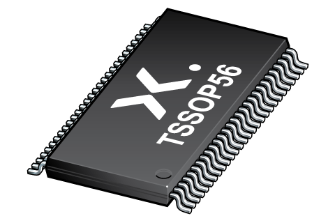
可訂購部件
| 型號 | 可訂購的器件編號 | 訂購代碼(12NC) | 封裝 | 從經銷商處購買 |
|---|---|---|---|---|
| 74ALVCH16500DGG | 74ALVCH16500DGG:11 | 935262542118 | SOT364-1 | 訂單產品 |

Register once, drag and drop ECAD models into your CAD tool and speed up your design.
Click here for more information18-bit universal bus transceiver; 3-state
The 74ALVCH16500 is an 18-bit universal transceiver with bus hold inputs and 3-state outputs. Data flow in each direction is controlled by output enable (OEAB and OEBA), latch enable (LEAB and LEBA), and clock (CPAB and CPBA) inputs. For A-to-B data flow, the device operates in the transparent mode when LEAB is HIGH. When LEAB is LOW, the A data is latched if CPAB is held at a HIGH or LOW logic level. If LEAB is LOW, the A-bus data is stored in the latch/flip-flop on the HIGH-to-LOW transition of CPAB. When OEAB is HIGH, the outputs are active. When OEAB is LOW, the outputs are in the high-impedance state.
Data flow for B-to-A is similar to that of A-to-B but uses OEBA, LEBA and CPBA. The output enables are complimentary (OEAB is active HIGH, and OEBA is active LOW). This device is fully specified for partial power down applications using IOFF. The IOFF circuitry disables the output, preventing the potentially damaging backflow current through the device when it is powered down.
Wide supply voltage range from 1.65 V to 3.6 V
CMOS low power dissipation
MULTIBYTE? flow-through standard pin-out architecture
Low inductance multiple VCC and GND pins for minimum noise and ground bounce
Direct interface with TTL levels (2.7 V to 3.6 V)
Bus hold on data inputs
Latch-up performance exceeds 100 mA per JESD 78 Class II Level B
Output drive capability 50 Ω transmission lines at 85 °C
Current drive ±24 mA at 3.0 V
Complies with JEDEC standards:
JESD8-7 (1.65 V to 1.95 V)
JESD8-5 (2.3 V to 2.7 V)
JESD8C/JESD36 (2.7 V to 3.6 V)
ESD protection:
HBM: ANSI/ESDA/JEDEC JS-001 class 2 exceeds 2000 V
CDM: ANSI/ESDA/JEDEC JS-002 class C3 exceeds 1000 V
Specified from -40 °C to +85 °C
| 型號 | VCC(A) (V) | VCC(B) (V) | Logic switching levels | Output drive capability (mA) | tpd (ns) | Nr of bits | fmax (MHz) | Power dissipation considerations | Tamb (°C) | Rth(j-a) (K/W) | Package name |
|---|---|---|---|---|---|---|---|---|---|---|---|
| 74ALVCH16500DGG | n.a. | n.a. | TTL | ± 24 | 2.9 | 18 | 150 | low | -40~85 | 93 | TSSOP56 |
| 型號 | 可訂購的器件編號,(訂購碼(12NC)) | 狀態 | 標示 | 封裝 | 外形圖 | 回流焊/波峰焊 | 包裝 |
|---|---|---|---|---|---|---|---|
| 74ALVCH16500DGG | 74ALVCH16500DGG:11 (935262542118) |
Active | ALVCH16500 |

TSSOP56 (SOT364-1) |
SOT364-1 |
SSOP-TSSOP-VSO-WAVE
|
SOT364-1_118 |
| 文件名稱 | 標題 | 類型 | 日期 |
|---|---|---|---|
| 74ALVCH16500 | 18-bit universal bus transceiver; 3-state | Data sheet | 2024-06-28 |
| SOT364-1 | 3D model for products with SOT364-1 package | Design support | 2020-01-22 |
| alvch16500 | alvch16500 IBIS model | IBIS model | 2013-04-08 |
| Nexperia_package_poster | Nexperia package poster | Leaflet | 2020-05-15 |
| SOT364-1 | plastic, thin shrink small outline package; 56 leads; 0.5 mm pitch; 14 mm x 6.1 mm x 1.2 mm body | Package information | 2022-06-23 |
| SOT364-1_118 | TSSOP56; Reel pack for SMD, 13"; Q1/T1 product orientation | Packing information | 2020-04-21 |
| 74ALVCH16500DGG_Nexperia_Product_Reliability | 74ALVCH16500DGG Nexperia Product Reliability | Quality document | 2025-03-20 |
| SSOP-TSSOP-VSO-WAVE | Footprint for wave soldering | Wave soldering | 2009-10-08 |
The Nexperia Longevity Program is aimed to provide our customers information from time to time about the expected time that our products can be ordered. The NLP is reviewed and updated regularly by our Executive Management Team. View our longevity program here.
| 文件名稱 | 標題 | 類型 | 日期 |
|---|---|---|---|
| alvch16500 | alvch16500 IBIS model | IBIS model | 2013-04-08 |
| SOT364-1 | 3D model for products with SOT364-1 package | Design support | 2020-01-22 |
| 型號 | Orderable part number | Ordering code (12NC) | 狀態 | 包裝 | Packing Quantity | 在線購買 |
|---|---|---|---|---|---|---|
| 74ALVCH16500DGG | 74ALVCH16500DGG:11 | 935262542118 | Active | SOT364-1_118 | 2,000 | 訂單產品 |
作為 Nexperia 的客戶,您可以通過我們的銷售機構訂購樣品。
如果您沒有 Nexperia 的直接賬戶,我們的全球和地區分銷商網絡可為您提供 Nexperia 樣品支持。查看官方經銷商列表。
The interactive datasheets are based on the Nexperia MOSFET precision electrothermal models. With our interactive datasheets you can simply specify your own conditions interactively. Start by changing the values of the conditions. You can do this by using the sliders in the condition fields. By dragging the sliders you will see how the MOSFET will perform at the new conditions set.