Register once, drag and drop ECAD models into your CAD tool and speed up your design.
Click here for more information74LVCV2G66DP
Overvoltage tolerant bilateral switch
The 74LVCV2G66 is a low-power, low-voltage, high-speed Si-gate CMOS device.
The 74LVCV2G66 provides two single pole single throw analog or digital switches. Each switch includes an overvoltage tolerant input/output terminal (pin nZ), an output/input terminal (pin nY) and low-power active HIGH enable input (pin nE).
The overvoltage tolerant switch terminals allow the switching of signals in excess of VCC. The low-power enable input eliminates the necessity of using current limiting resistors in portable applications when using control logic signals much lower than VCC. These inputs are also overvoltage tolerant.
Features and benefits
Wide supply voltage range from 2.3 V to 5.5 V
Ultra low-power operation
Very low ON resistance:
8.0 Ω (typical) at VCC = 2.7 V
7.5 Ω (typical) at VCC = 3.3 V
7.3 Ω (typical) at VCC = 5.0 V.
5 V tolerant input for interfacing with 5 V logic
High noise immunity
Switch handling capability of 32 mA
CMOS low-power consumption
Latch-up performance exceeds 250 mA
Incorporates overvoltage tolerant analog switch technology
Switch accepts voltages up to 5.5 V independent of VCC
ESD protection:
HBM: ANSI/ESDA/JEDEC JS-001 class 2 exceeds 2000 V
CDM: ANSI/ESDA/JEDEC JS-002 class C3 exceeds 1000 V
Specified from -40 °C to +85 °C and -40 °C to +125 °C
參數類型
| 型號 | Package name |
|---|---|
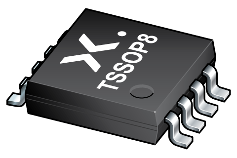
| 74LVCV2G66DP | TSSOP8 |
封裝
下表中的所有產品型號均已停產 。
| 型號 | 可訂購的器件編號,(訂購碼(12NC)) | 狀態 | 標示 | 封裝 | 外形圖 | 回流焊/波峰焊 | 包裝 |
|---|---|---|---|---|---|---|---|
| 74LVCV2G66DP | 74LVCV2G66DP,125 (935274431125) |
Obsolete | Y66 Standard Procedure Standard Procedure |

TSSOP8 (SOT505-2) |
SOT505-2 | SOT505-2_125 |
Series
文檔 (7)
| 文件名稱 | 標題 | 類型 | 日期 |
|---|---|---|---|
| 74LVCV2G66 | Overvoltage tolerant bilateral switch | Data sheet | 2023-08-29 |
| AN10161 | PicoGate Logic footprints | Application note | 2002-10-29 |
| AN11009 | Pin FMEA for LVC family | Application note | 2019-01-09 |
| Nexperia_document_guide_MiniLogic_PicoGate_201901 | PicoGate leaded logic portfolio guide | Brochure | 2019-01-07 |
| SOT505-2 | 3D model for products with SOT505-2 package | Design support | 2019-01-18 |
| Nexperia_package_poster | Nexperia package poster | Leaflet | 2020-05-15 |
| SOT505-2 | plastic, thin shrink small outline package; 8 leads; 0.65 mm pitch; 3 mm x 3 mm x 1.1 mm body | Package information | 2022-06-03 |
Longevity
The Nexperia Longevity Program is aimed to provide our customers information from time to time about the expected time that our products can be ordered. The NLP is reviewed and updated regularly by our Executive Management Team. View our longevity program here.
模型
| 文件名稱 | 標題 | 類型 | 日期 |
|---|---|---|---|
| SOT505-2 | 3D model for products with SOT505-2 package | Design support | 2019-01-18 |
How does it work?
The interactive datasheets are based on the Nexperia MOSFET precision electrothermal models. With our interactive datasheets you can simply specify your own conditions interactively. Start by changing the values of the conditions. You can do this by using the sliders in the condition fields. By dragging the sliders you will see how the MOSFET will perform at the new conditions set.