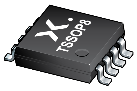
可訂購部件
| 型號 | 可訂購的器件編號 | 訂購代碼(12NC) | 封裝 | 從經(jīng)銷商處購買 |
|---|---|---|---|---|
| 74LVC2G241DP | 74LVC2G241DP,125 | 935272006125 | SOT505-2 | 訂單產(chǎn)品 |
進一步了解Nexperia的豐富產(chǎn)品組合,比如二極管、雙極性晶體管、ESD保護器件、MOSFET器件、氮化鎵場效應晶體管(GaN FET)、絕緣柵雙極晶體管(IGBT)以及模擬IC和邏輯IC。我們的器件廣泛應用于汽車、工業(yè)、移動和消費等多個領域,幾乎為世界上所有電子設計提供支持。

Register once, drag and drop ECAD models into your CAD tool and speed up your design.
Click here for more informationDual buffer/line driver; 3-state
The 74LVC2G241 is a dual non-inverting buffer/line driver with 3-state outputs. The 3-state outputs are controlled by the output enable inputs 1OE and 2OE:
A HIGH level at pin 1OE causes output 1Y to assume a high-impedance OFF-state.
A LOW level at pin 2OE causes output 2Y to assume a high-impedance OFF-state.
Schmitt trigger action at all inputs makes the circuit highly tolerant of slower input rise and fall times.
Inputs can be driven from either 3.3 V or 5 V devices. This feature allows the use of the 74LVC2G241 as a translator in a mixed 3.3 V and 5 V environment.
This device is fully specified for partial power-down applications using IOFF. The IOFF circuitry disables the output, preventing a damaging backflow current through the device when it is powered down.
Wide supply voltage range from 1.65 V to 5.5 V
5 V tolerant input/output for interfacing with 5 V logic
High noise immunity
±24 mA output drive (VCC = 3.0 V)
CMOS low power consumption
Latch-up performance exceeds 250 mA
Direct interface with TTL levels
Inputs accept voltages up to 5 V
Complies with JEDEC standard:
JESD8-7 (1.65 V to 1.95 V)
JESD8-5 (2.3 V to 2.7 V)
JESD8-B/JESD36 (2.7 V to 3.6 V)
ESD protection:
HBM: ANSI/ESDA/JEDEC JS-001 class 2 exceeds 2000 V
CDM: ANSI/ESDA/JEDEC JS-002 class C3 exceeds 1000 V
Multiple package options
Specified from -40 °C to +85 °C and -40 °C to +125 °C
| 型號 | VCC (V) | Logic switching levels | Output drive capability (mA) | fmax (MHz) | Nr of bits | Power dissipation considerations | Tamb (°C) | Rth(j-a) (K/W) | Rth(j-c) (K/W) | Package name |
|---|---|---|---|---|---|---|---|---|---|---|
| 74LVC2G241DP | 1.65?-?5.5 | CMOS/LVTTL | ± 32 | 175 | 2 | low | -40~125 | 220 | 107 | TSSOP8 |
| Model Name | 描述 |
|---|---|
|
|
| 型號 | 可訂購的器件編號,(訂購碼(12NC)) | 狀態(tài) | 標示 | 封裝 | 外形圖 | 回流焊/波峰焊 | 包裝 |
|---|---|---|---|---|---|---|---|
| 74LVC2G241DP | 74LVC2G241DP,125 (935272006125) |
Active | V241 |

TSSOP8 (SOT505-2) |
SOT505-2 | SOT505-2_125 |
| 文件名稱 | 標題 | 類型 | 日期 |
|---|---|---|---|
| 74LVC2G241 | Dual buffer/line driver; 3-state | Data sheet | 2024-04-30 |
| AN10161 | PicoGate Logic footprints | Application note | 2002-10-29 |
| AN11009 | Pin FMEA for LVC family | Application note | 2019-01-09 |
| Nexperia_document_guide_MiniLogic_PicoGate_201901 | PicoGate leaded logic portfolio guide | Brochure | 2019-01-07 |
| SOT505-2 | 3D model for products with SOT505-2 package | Design support | 2019-01-18 |
| lvc2g241 | 74LVC2G241 IBIS model | IBIS model | 2014-10-20 |
| Nexperia_package_poster | Nexperia package poster | Leaflet | 2020-05-15 |
| SOT505-2 | plastic, thin shrink small outline package; 8 leads; 0.65 mm pitch; 3 mm x 3 mm x 1.1 mm body | Package information | 2022-06-03 |
| SOT505-2_125 | TSSOP8; Reel pack for SMD, 7''; Q3/T4 product orientation | Packing information | 2020-04-21 |
| 74LVC2G241DP_Nexperia_Product_Reliability | 74LVC2G241DP Nexperia Product Reliability | Quality document | 2025-03-20 |
The Nexperia Longevity Program is aimed to provide our customers information from time to time about the expected time that our products can be ordered. The NLP is reviewed and updated regularly by our Executive Management Team. View our longevity program here.
| Model Name | 描述 |
|---|---|
|
|
| 型號 | Orderable part number | Ordering code (12NC) | 狀態(tài) | 包裝 | Packing Quantity | 在線購買 |
|---|---|---|---|---|---|---|
| 74LVC2G241DP | 74LVC2G241DP,125 | 935272006125 | Active | SOT505-2_125 | 3,000 | 訂單產(chǎn)品 |
作為 Nexperia 的客戶,您可以通過我們的銷售機構(gòu)訂購樣品。
如果您沒有 Nexperia 的直接賬戶,我們的全球和地區(qū)分銷商網(wǎng)絡可為您提供 Nexperia 樣品支持。查看官方經(jīng)銷商列表。
The interactive datasheets are based on the Nexperia MOSFET precision electrothermal models. With our interactive datasheets you can simply specify your own conditions interactively. Start by changing the values of the conditions. You can do this by using the sliders in the condition fields. By dragging the sliders you will see how the MOSFET will perform at the new conditions set.